Difference Between Avalanche Breakdown and Zener Breakdown

What is Avalanche Breakdown?
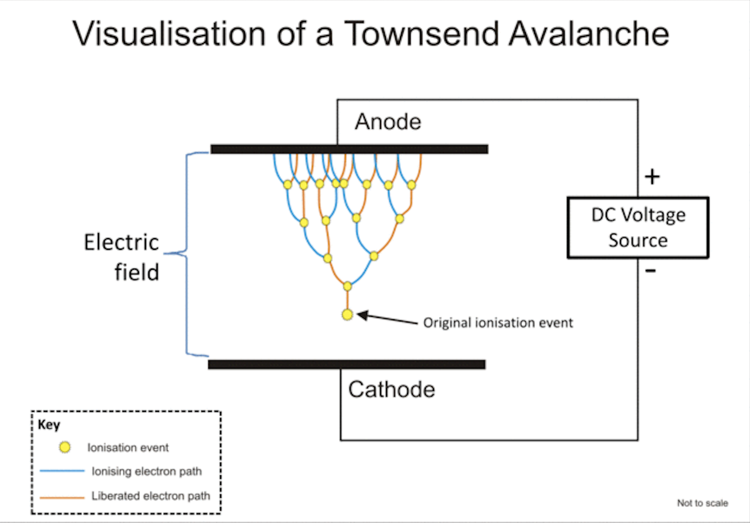
The foremost root for the avalanche breakdown is what we call “avalanche effect”. This takes place when significantly high reverse bias voltage causes the broadening of the depletion region. This process, in turn makes the electric field considerably strong. The minority charge carriers speed up in this depletion region and gain kinetic energy. The electrons found in the valance band are knocked off when the field is considerably strong. This results in the creation of a hole and an electron, which is a conduction electron. This further leads to an energetic electron, which may be considered a hole, being able to yield two or more charge carriers. When put in simpler terms, this means that an increase is similar to an avalanche based on the exponential nature. However, as a result, the impact ionization causes heat within which can result in potential damage to the diode which might destroy the diode altogether.

What is Zener Breakdown?
Zener breakdown, on the other hand, takes place when the doping concentration is elevated on the scale by a great extent. This leads to the depletion region widening by a little number of atoms. The electric field, however becomes substantially strong, yet remains narrow. Thus, many charge carriers cannot get accelerated. Instead, a quantum mechanical effect is undertaken. This phenomenon is recognized as quantum tunneling. The ionization happens without any impact. As a result, the electrons are able to just tunnel through.
Tunneling Effect
This occurs when insulator separates two distinct pieces of a conductor. The order of the nanometers and the thickness of the insulator are equivalent to another. A rise in the given current is observed, whereby the electrons conduct. Despite the first instinct to believe that the flow of current would be blocked by an insulator, it can be observed that the electrons are able to pass through the insulators as a result of the damage. This act makes it seem as if the electrons have vanished, or simply relocated from one side and have appeared on the other side. In conclusion, it can be said that the wave nature of electrons enables this process.
Despite being different, the two breakdowns share a similarity. Both mechanisms release free charge carriers in the depletion region. This causes the diode to conduct when reverse biased.
However, both mechanisms differ based on a variety of reasons, which primarily low in the quantum mechanical aspect of the breakdowns. The differences are defined in the following text:
Process
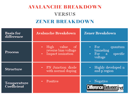
The process of Avalanche breakdown predominantly involves a phenomenon known as impact ionization. Owing to a high reverse-bias field, the motion of minority carriers through the junction is encouraged. While there is a substantial increase in the reverse bias voltage, the velocity of carriers crossing the junction subsequently increases. This in turn causes them to produce more carriers by eliminating electrons and holes from the crystal lattice. The occurrence of quantum tunneling, that brings along the high electric field causing electron-hole pairs to be pulled from the covalent bonds. As a result, they cross the intersection. This process occurs for a specific voltage when the combined field due to the immobile ions in depletion region and the reverse bias collectively become abundant to impact Zener breakdown.
Structure
The diode which break down, in case of avalanche breakdown, are generally p-n junction diode which are normally doped. Nevertheless, Zener diodes contain highly doped n and p regions, resulting in a thin depletion region and a very high electric field across the depletion region.
Temperature Coefficient
Positive temperature coefficient is experienced by Avalanche breakdowns, while on the other hand, Zener causes the voltage to break down, thus resulting in a negative temperature coefficient.
Difference between Avalanche Breakdown and Zener Breakdown: Comparison Chart

Search DifferenceBetween.net :
Leave a Response
References :
[0]Circuits Today. PN junction breakdown characteristics. 19 December 2013. 22 April 2018.
[1]Kruger, Anton. Zener and Avalanche Breakdown/Diodes. 18 October 2001. 22 April 2018.
[2]Zeghbroeck, B. Van. p-n Junctions. 2011. 2018.
[3]Image credit: https://upload.wikimedia.org/wikipedia/commons/thumb/a/ac/Electron_avalanche.gif/640px-Electron_avalanche.gif
[4]Image credit: https://upload.wikimedia.org/wikipedia/commons/thumb/5/5a/I-V_curve_for_a_Zener_Diode.svg/581px-I-V_curve_for_a_Zener_Diode.svg.png
